


News and Information
The assembly process for DIP components on a PCB
2025-12-08
General Introduction to DIP Component Assembly on PCBs
A brief explanation of DIP components.
DIP (Dual In-line Package) is a type of electronic component packaging in which the component's leads are arranged in two parallel rows and designed to be inserted through holes on a PCB (Printed Circuit Board). After being mounted onto the PCB, the DIP component's leads are soldered permanently using Through-Hole Technology (THT), creating a robust electrical and mechanical connection that ensures stable signal transmission and enhances the durability of the circuit.
DIP components come in various types with different numbers of pins, ranging from DIP8, DIP14, DIP28 to DIP40, depending on the complexity of the electronic circuit. They are widely used in integrated circuits (ICs), amplifiers, microcontrollers, ROM and RAM memory, and high-power devices.
The Importance of DIP Assembly on PCBs
Although SMT technology is gradually dominating the electronic component manufacturing market, PCBs still play an indispensable and crucial role in many industrial applications. Assembling DIP components onto PCBs not only enhances mechanical durability but also ensures flexible repairability and meets the high-power requirements of modern electronic systems.
High durability & secure connection
PCBs are designed to securely mount electronic components, providing excellent vibration resistance, high thermal stability, and minimizing physical impacts. DIP components, when mounted onto PCBs using Through-Hole Technology (THT), create a robust mechanical connection—making them particularly well-suited for devices operating in environments with severe vibrations or high temperatures, such as military equipment, aerospace systems, or industrial automation applications.
Easy repair & maintenance capability
Unlike SMT, where small and difficult-to-handle components are used, PCBs with DIP components make the repair process much simpler. When a component fails, technicians can easily remove and replace it without needing sophisticated specialized soldering equipment. This is especially crucial in industrial electronic systems, where rapid repair times help minimize production disruptions and reduce operating costs.
Well-suited for high-power devices
Devices requiring high power and large currents, such as power supplies, amplifiers, and industrial electrical systems, still prioritize the use of DIP components on PCBs. The robust through-hole connections optimize electrical conductivity, minimize energy losses, and ensure stable performance over the long term. This is a crucial factor that enables PCBs to maintain their leading position in applications demanding high durability and performance.
DIP Component Assembly Process on PCB
Assembling DIP (Dual In-line Package) components onto a PCB (Printed Circuit Board) is an important step in electronic manufacturing. This process consists of five main steps, from component preparation to final quality inspection, aimed at ensuring the accuracy, stability, and operational performance of the circuit.
1. Prepare DIP Components & PCB
Before proceeding with assembly, it is necessary to thoroughly prepare both DIP components and the PCB board to ensure soldering accuracy and quality.
✔ Choose the appropriate PCB: The PCB must have dimensions and a number of layers that match the circuit design and also meet manufacturing standards.
✔ Inspect DIP components: Remove components with bent, oxidized, or defective pins to prevent interference with the soldering process.
✔ Component foot placement: Accurately identify the positions of the holes on the PCB to ensure proper component insertion and avoid soldering errors.
2. Solder DIP Components onto the PCB
After preparation is complete, the DIP components will be inserted into the circuit board in their correctly designed positions.
✔ Insert components according to the correct specifications: Ensure that component pins pass through the PCB holes accurately and without any misalignment.
✔ Use component holding clips: Secure components to prevent them from falling or shifting out of position during soldering, especially in mass production.
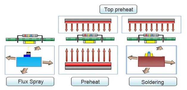
3. Soldering DIP Components onto the PCB
There are two main methods for soldering DIP components onto PCBs, depending on the production scale and technical requirements.
✔ Hand soldering: Uses an electric soldering iron and solder wire to secure components. Suitable for small-scale production or repairs.
✔ Soldering by machine: The PCB is passed through a bath of molten solder, enabling rapid, simultaneous soldering of component leads—ideal for mass production.
✔ Solder joint inspection: Ensure that the solder spreads evenly, there is no solder deficiency, cold solder joints, or short circuits between component leads.
4. Trim the Component Leads & Clean the PCB
After soldering is complete, it is necessary to remove the excess leads and clean the PCB to ensure stable circuit signal operation.
✔ Trim component leads: Use specialized cutting pliers to neatly trim excess leads, avoiding damage to other PCB layers.
✔ PCB cleaning: Remove soldering flux residues using a specialized solution to prevent contamination and ensure the durability of the circuit board.
5. Quality Control (QC)
The final step is quality control (QC) to ensure the circuit operates accurately.
✔ Automated Optical Inspection (AOI): Detects soldering defects, misaligned component leads, or missing solder joints.
✔ Electrical Testing: Measure resistance, voltage, and check the conductivity of each component to ensure proper operation.
Practical Applications of DIP Component Assembly
Although SMT soldering technology is now dominant in modern electronics manufacturing, DIP component assembly still plays an important role in many fields thanks to its high mechanical durability, excellent load-bearing capacity, and ease of maintenance. Below are some common real-world applications of this technology:
- High-power devices: DIP components are commonly used in power supplies, amplifiers, military equipment, and systems requiring high current. Thanks to their robust through-hole soldering connections, these components can withstand harsh environments and intense vibrations without compromising operational performance.
- Easy to Maintain and Repair: In industrial control circuits and telecommunications systems, DIP components are easier to replace than SMT components. Thanks to their through-hole PCB pin design, technicians can remove and replace faulty components without needing specialized soldering equipment, thereby optimizing maintenance time and reducing repair costs.
- DIP component assembly line: In large-scale electronics factories, DIP component assembly remains an important part of the manufacturing process. In particular, circuit boards using DIP components are commonly found in measuring devices, industrial control systems, and automotive electronic systems—applications that require long-term stability and easy component replacement when necessary.
Advantages & Disadvantages of Assembling DIP Components on PCBs
| Criteria | Advantages | Disadvantages |
| Connectivity & Mechanical Durability | Firm connection, excellent resistance to force and vibration. | Occupies more PCB area than SMT. |
| Repairability | Easy to replace components; no specialized soldering equipment required. | Difficult to mass-produce due to limited automation support. |
| Application in devices | Suitable for high-power devices such as power supplies, amplifiers, and military equipment. | Through-hole soldering requires more time than SMT. |
In general, DIP components remain a reliable choice for devices that require high mechanical durability, good load-bearing capacity, and easy component replacement when necessary. Thanks to their through-hole pin design, they ensure a robust connection, minimizing the risk of failure due to vibration or impact. However, DIP is not the optimal solution for mass production, as the assembly process involves many manual steps and takes more time compared to SMT technology. Moreover, compact devices or circuits with high component density typically do not use DIP components, as they occupy considerable space on the PCB.
Summary
Assembling DIP (Dual In-line Package) components onto PCBs remains an important technology in the electronics industry, especially for high-power devices that require mechanical durability and ease of maintenance. Although SMT (Surface Mount Technology) is becoming increasingly popular, DIP still holds advantages thanks to its excellent resistance to vibration, as well as its ease of repair and component replacement when necessary.
However, DIP is not the optimal choice for compact devices or mass production, as it requires a larger PCB area and the through-hole soldering process takes more time. Therefore, this technology is primarily used in power supplies, amplifiers, military equipment, telecommunications systems, and industrial production lines—places where durability and repairability are more important than compactness.
Although DIP is no longer the primary standard in modern electronics manufacturing, it remains an indispensable solution for certain specialized applications. A thorough understanding of the assembly process, advantages and disadvantages, and practical applications of this technology enables engineers and businesses to choose the most suitable manufacturing method for their specific needs.
Previous:
Contact Us
Contact Number:
+86 21 6088 8500
+86 4006 777 950
+86 150 2686 5822
Email:
marketing@hapoin.com
Headquarter Address:
6, South Metropolis Garden, No. 1165, Jindu Road, Minhang District, Shanghai
OUTLETS
Service Outlets

Shanghai-Head Office
Shanghai Hapoin Enterprise Development Co., Ltd.
Address: Building 6, Southern Metropolis Garden, No. 1165, Jindu Road, Minhang District, Shanghai
Telephone:+86 150 2686 5822
Email:info@hapoin.com
Shenzhen Branch
Shenzhen Hapoin Ruihe Technology Development Co., Ltd.
Address: Room 302, 3rd Floor, Building B, Kaicheng High-tech Park, Dalang Street, Longhua District, Shenzhen
Telephone:+86 0755 2223 2285
Email:sales@hapoin.com
Hong Kong Branch
HAPOIN ENTERPISE LIMITED
Address: Unit 917A, 9/F., Tower A, New Mandarin Plaza, No. 14 Science Museum Road
Telephone:+00852 61187991
Email:sales@hapoin.com
Vietnam Branch
HAPOIN VIETNAM
Address: 6th Floor, CTM Office Building, No. 139, Zhipiao Road, Zhipiao District, Hanoi, Vietnam
Telephone:+84 398 848 969
Email:sales@hapoin.com
Japan Branch
HAPOIN CO., LTD.
Address: 6th Floor, 2-3-8 Iwamotocho, Chiyoda-ku, Tokyo
Telephone:+81 070 9356 1267
Email:sales@hapoin.com
Kunshan Office
Kunshan Office
Address: 10th Floor, Building B, Modern Plaza, No. 8, Weiye Road, Yushan Town, Kunshan City
Telephone:+86 150 2686 5822
Email:sales@hapoin.com
Taipei Branch
Uniwin Chemical Co.,LTD.
Address: No. 14, Alley 3, Lane 250, Section 2, Huanhe South Road, Taipei 10853
Telephone:+886 02 2336 2202
Email:sales@hapoin.com
Beijing Office
Beijing Office
Address: Room 306, Building 4, Zhongtou Oriental, West Zhihe North, Chaoyang District, Beijing
Telephone:+86 150 2686 5822
Email:sales@hapoin.com


Contact Number
Headquarter Address
6, South Metropolis Garden, No. 1165, Jindu Road, Minhang District, Shanghai
Follow the official account
Follow the video account

